PSpice Examples for EE-253 PSpice allows the user to model semiconductor devices such as diodes, bipolar junction transistors (BJT), field effect transistors, and integrated circuits such as operational amplifiers. We discuss here only very simple models for the diode and BJT. Please refer to a PSpice manual for full details on these and other semiconductor devices and circuits. The resistor, capacitor, and inductor are each adequately described with a single parameter. However, semiconductors are usually described with many parameters. For example, the diode model in PSpice has 14 parameters, while the BJT model has 40 parameters! In addition, many electronic circuits contain several of the same diodes or transistors. For these reasons, semiconductor devices are described with two statements. The circuit statement gives the device, the nodes that are connected to, and a model name. A separate model definition lists the device parameters. Therefore, if there are two or more of the same diodes in a circuit, each diode circuit description statement uses the same model name. Only one model definition is then needed. Although PSpice allows the user to describe diodes, BJTs, etc. with many parameters, it is often not necessary to explicitly list all of them. PSpice contains default values for all parameters. In essence, PSpice has built-in generic models for semiconductor devices. You only need to specify those parameter values that are different than the default values. Diodes
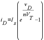
The diode is a two terminal device that essentially allows current conduction in only one direction. The basic low frequency diode current-voltage relationship is given by The thermal voltage, VT, is approximately 26 mV at room temperature, so we usually only need to specify the saturation current, IS (PSpice default is IS = 10-15 A).
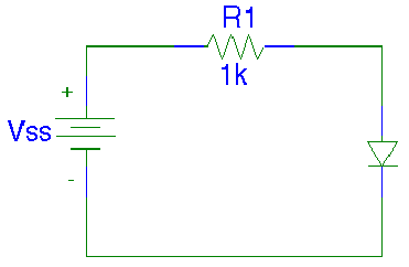
Use PSpice to find the diode current and voltage in the circuit shown
The supply voltage is 2 V, and the current limiting resistor R1 = 1KW . The diode parameters are IS = 2.6 x 10⁻¹⁵ A, VT = 26mV, and n = 1. We construct the following schematic using the part Dbreak for the diode. An Iprobe is inserted in the circuit to display the current and a Viewpoint is used to obtain the diode voltage. (In place of Iprobe and Viewpoint you can enable or disable the bias voltages and currents by using the toolbar button V and I).
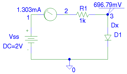
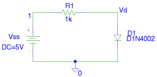
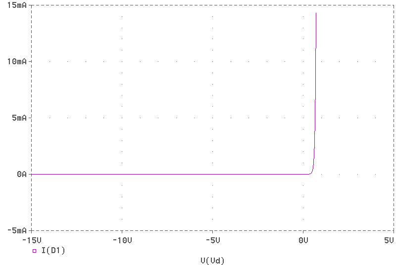
We must now define the model for the diode. Using the left mouse button select the diode symbol (Symbol should turn red). From the Edit Menu select Model. The dialog box appears with the following items. Change model Reference… Edit Instant Model(Text)… Edit Instant Model(parts)… The button Change model Reference… will allow us to change the model from Dbreak to another model name. The Edit Instant Model(Text)… will allow us to create the parametrs of the new model. The Edit Instant Model(parts)… will allow us to edit a previously defined model with the intent of creating a new model. Click the Change model Reference button and change the model name Dbreak to a new model called Dx. Next click the Edit Instant Model(Text)… and change the saturation current to Is = 2.6e-15. Click the OK button to accept the model. The only parameter that we have changed is Is. Notice that the diode model name has changed from Dbreak to Dx. Upon simulation we see that the diode current is 1.303 mA, and the diode voltage is 696.79mV. Use PSpice to obtain the i-v characteristic of the diode with model number D1N4002. Sweep the input voltage from -15 V to 15 V. Construct the following schematic. Select the setup from the analysis menu, click the DC Sweep dialog button. The DC sweep dialog box appears. For the Sweep variable type select the voltage source, and set its name to Vss. Using the sweep type linear, set the starting value to -15, end value to 15 and increment to 0.1.
When simulation is complete probe graphic window appears. Add the trace I(D1). This is the trace of the diode current versus the supply voltage Vss. We need to change the x-axis variable to V(Vd) to obtain the plot of diode current versus diode voltage. To do this from the Plot pull-down menu select X Axis Settings, click the Axis Variable button to open the variable list, and select V(Vd) to be the horizontal axis. Click OK button and the diode i-v characteristic is displayed as shown.
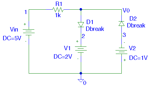
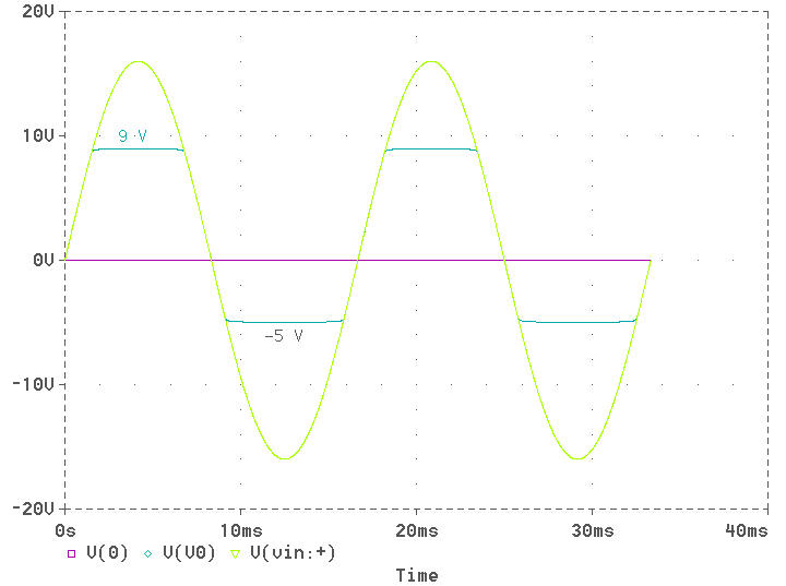
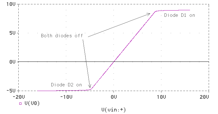
In the circuit below determine V0 as Vin is varied from -5 to +5 V. The two diodes are identical and have a saturation current of IS = 10-15A.
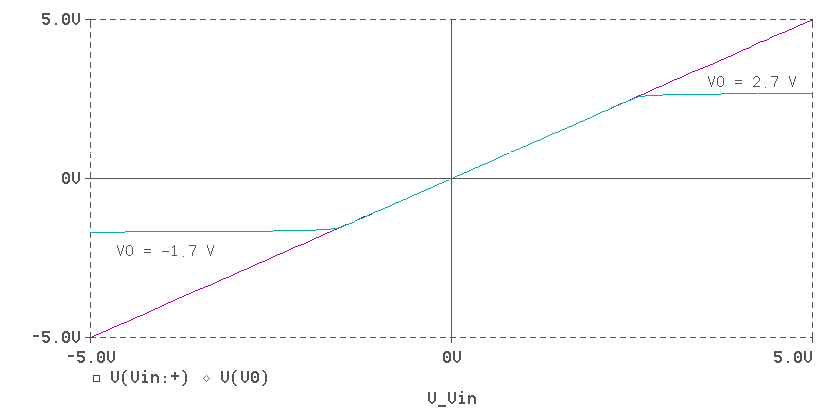
The circuit is known as a diode limiter. When D1 is shorted, the output voltage is 2V. When D2 is shorted, the output voltage is -1 V. This circuit therefore, limits the output voltage between -1 and 2 V. Actually there is a voltage drop of approximately 0.7 V across the diode. This means we should expect the output voltage to vary approximately between -1.7 V to 2.7 V. In the probe, the input voltage V(Vin), and the output voltage V(V0) are plotted as shown.
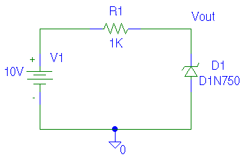
Obtain the I-v characteristic of the Zener diode (D1N750 is a 4.7 V Zener). The voltage regulator circuit shown below has R = 1 KW and uses Zener diode D1N750.
When simulation is complete probe graphic window appears. From the Plot pull-down menu select X Axis Settings, click the Axis Variable button to open the variable list, and select V(Vout) to be the horizontal axis. Click OK button and the Zener diode i-v characteristic is displayed as shown.
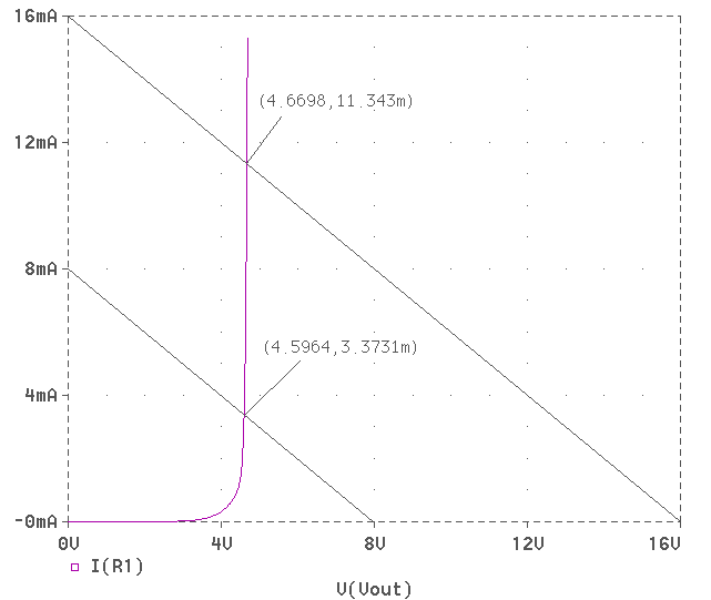
Now we can draw the load lines corresponding to V1 = 16 V, and V1 = 8 V. From KVL we have
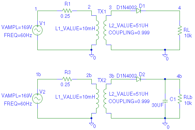
(a) When i = 0, Vout = V1 = 16 V and when Vout = 0, i = 16/1000 = 16 mA In Probe from Tools pull-down menu select Label/Line and draw the above line. Enable the Cursor and move the operating point and from the Tools select Label/Mark to mark the coordinates of the operating point. The output voltage is found to be 4.6698 V. ( b) Repeat (a) for V1 = 6 V. The output voltage is found to be 4.5964 V. This represent a drop in the output voltage of less than 1.57 percent when the input voltage is changed form 16 V to 8 V. A half-wave diode circuit with a step down transformer of turn ratios 14:1 is supplying a load RL = 10 KW as shown. The diode model is 1N4002. The supply voltage amplitude is 169 V, and its frequency is 60Hz. Use transient analysis to plot the voltage across RL.
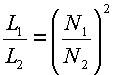
In PSpice we can model a transformer by letting the coupling coefficient approach 1 (Approx 0.999) and by making L1 and L2 large enough so that w L1 and w L2 are greater than other reactances in the circuit. The property of an ideal transformer result in
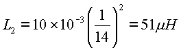
In PSpice set K = 0.999, L1 = 10mH, then
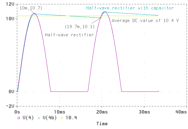
Since in PSpice we cannot have a loop of only inductor and voltage source, a small resistance is added to prevent an error. This can represent the primary winding resistance. After setting the first schematic enable the transient analysis. Use a Final Time of 33.33ms (to represent two cycles) and a small Ceiling value of 0.01ms. In the second Schematic a 30 m F capacitor is used to obtain a DC output voltage of a small ripple. Simulate and in Probe add traces V(4) and V(4b). The result is as shown. The average DC value for the circuit with the capacitor is approximately 10.4 V.
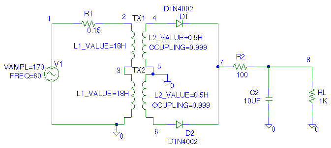
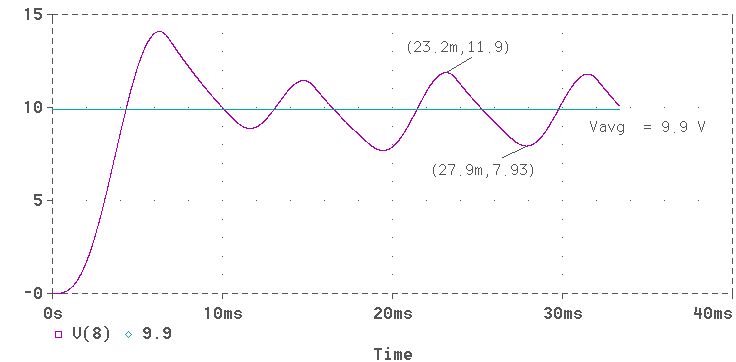
A full-wave diode circuit with a center-tapped step down transformer of turn ratios 6:1 is supplying a load RL = 1 KW as shown. A 10 m F capacitor is added to smooth the ripple. R2 is added to provide a voltage divider so as to control the voltage across RL. The diode model is 1N4002. The supply voltage amplitude is 169 V, and its frequency is 60Hz. Use transient analysis to plot the voltage across RL.
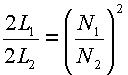
Two transformers (XFRM_Linear) are used to represent a center-tapped transformer. The ratio of self-inductances is given by
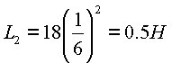
Let L1 =18H, then
and we use a coupling coefficient of 0.999. Since in PSpice we cannot have a loop of only inductor and voltage source, a small resistance is added to prevent an error. This can represent the primary winding resistance. After setting the first schematic enable the transient analysis. Use a Final Time of 33.33ms (to represent two cycles) and a small Ceiling value of 0.01ms. The result is as shown.
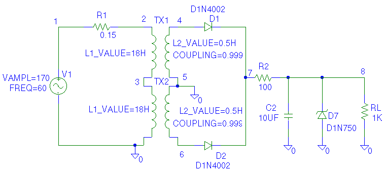
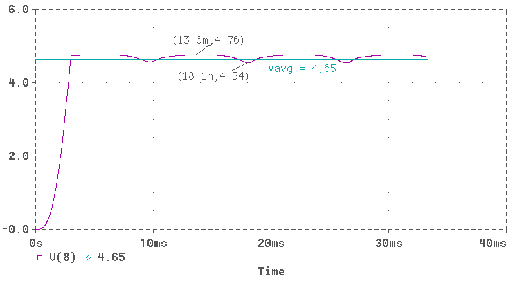
A Zener diode (1N750) is added to the circuit of Example 7 to have a 4.7 V regulated DC power supply. Use transient analysis to plot the voltage across RL. The Zener diode 1N750 has a breakdown voltage of 4.7 V.
The result is as shown.
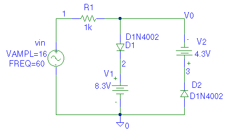
Design a clipper circuit to clip off the portion of an input voltage that falls above 9 V or below -5 V. Use 1N4002 diodes which has a voltage drop of approximately 0.7 V. V1 = 9 - 0.7 = 8.3 V, V2 = 5 - 0.7 = 4.3 V. The input is a sine wave of 16 V amplitude and 60 Hz frequency. R1 = 1K to limit the forward diode current. Use transient analysis with a final time of 33.33 ms and a step ceiling of 0.01ms. Plot the input and output voltage waveform. On a separate graph obtain plot the transfer characteristic Vo versus vin.
The result is shown.
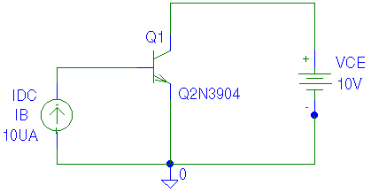
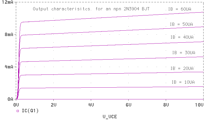
Using PSpice, obtain the output characteristics (ic versus vce ) for an npn 2N3904 BJT. The base-emitter junction is forward biased with a DC current source and the collector-base junction is reversed biased by a DC voltage source connected between the collector and emitter. We use the DC analysis and we need to set up the DC sweep. The dialog box is opened and for the main Sweep variable we type VCE , and the linear sweep is set from 0 to 10 V in increments of 0.01 V. The Nested Seep button is clicked to open its dialog box, and for the Nested Sweep variable we type iB , and we use a linear seep from 0 to 60 m A in increment of 10 m A. In Probe we add the trance IC(Q1) and obtain the following output characteristics.
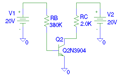
The simplest type of biasing for a bipolar transistor is the base biased circuit shown below. (a) Assuming b = 165, and ,
(b) Using PSpice run a DC bias point solution and determine the Q-point values and
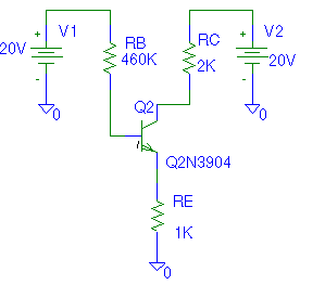
For the fixed bias configuration shown below, determine the Q point by hand and find (5.08 mA, 4.72 V, -4.01 V)
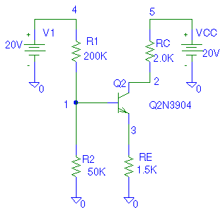
(b) Using PSpice run a DC bias point solution and determine the Q-point values and The most popular biasing is the voltage-divider biasing shown below, determine the Q
point by hand and find
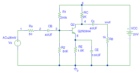
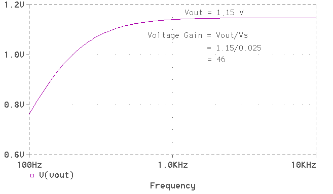
(b) Using PSpice run a DC bias point solution and determine the Q-point values and For the 2N3904 BJT transistor amplifier circuit shown, perform an AC analysis in decade variation from 100 Hz to 10 KHz with 500 points per decade. VS = 25mV AC ( Use VSRC). Use Probe to obtain the output voltage Vout. Find the voltage Gain.
The result is as shown.
|