PSpice Examples for EE-230
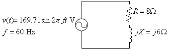
Part 1 AC Power and Three-phase Circuits For the
circuit shown, use PSpice and Probe to graph the instantaneous voltage, current
and power over one cycle.
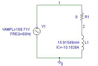
The initial
current in the inductor is given to be -10.1826 A. The reactor inductance is
.
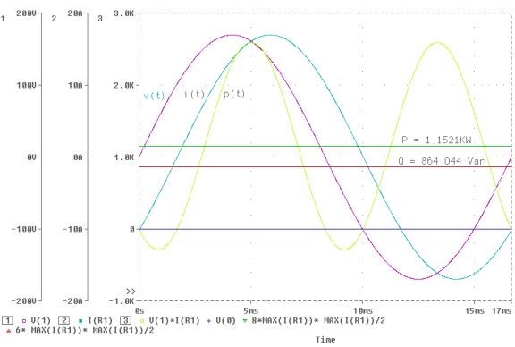
Select Transient
analysis, set the final time to 16.6667 ms, and the Step Ceiling to 0.01
ms. In Probe plot the instantaneous voltage V(1), and from Plot add Y-axis and
the trace for current I(R1). Repeat to add the Y-axis and the trace for the
instantaneous power p (t), (in probe for trace expression type V(1)*I(R1)).
The real
power can be expressed as
Select the
power axis and add the traces with Trace Expressions as
8*MAX(I(R1))*MAX(I(R1))/2, and 6*MAX(I(R1))*MAX(I(R1))/2 to display P and Q.
* Schematics Netlist *
L_L1 2 0 15.91549mH IC=-10.1826A
R_R1 1 2 8
V_V1 1 0 +SIN 0 169.71V 60Hz 0 0 0
The result
is shown in the next page.
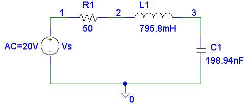
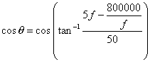
For the
circuit shown, use PSpice and Probe to graph the real and reactive powers
delivered to the circuit as a function of frequency. Use the AC analysis to
sweep the source frequency from 300 Hz to 500 Hz in steps of 1 Hz and Probe to
obtain one graph showing real and reactive power supplied by the source and
another graph showing power factor as a function of frequency. Determine the source frequency for unity
power factor.
* Schematics Netlist *
R_R1 1 2 50
V_Vs 1 0 AC 20V
L_L1 2 3 795.8mH IC=0
C_C1 3 0 198.94nF IC=0
The circuit
impedance is
The real power
is
and the
reactive power is
The power factor is
In probe,
select Plot control and Add Plot to create two graphs on the
screen. Select X-axis and set the range
to change the frequency axis scale to 350 450 Hz. Using Add Trace plot P and Q with the trace expressions
given by (2) and (3).
Use Plot
Control, select plot and down key to switch to the lower graph and using Add
Trace add the power factor with the Trace Expression as given by (4). Using the cursor command you can move along
the plot with the right or left arrows. The co-ordinates at which the cursor is
located are displayed on the lower right hand of the screen. You can select
between different plots by holding down the control key while pressing the
right or left arrow keys. Using the Label command you can add text, lines and arrows to the plot. The plot produced on
the probe is shown below. From the
plots we see that the circuit changes from capacitive to inductive at the
series resonance frequency where reactive power is zero.
At unity
power factor frequency, f = 400 Hz, P = 4 W
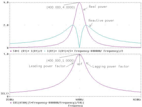
A 3-phase
line has an impedance of 3 + j4 W. The line feeds two balanced three-phase loads that are connected in
parallel. The first load is Y-connected
and has an impedance of 30 + j40 W/phase. The second load is delta connected
and has an impedance of 60 - j45 W/phase. The line is
energized at the sending-end from a 3-phase balanced supply of line to neutral
voltage
(a)
Current in
the line for each phase.
(b)
Current in
each phase of the Y-connected loads.
(c)
Current in
each phase of the delta connected loads.
The line inductance per phase is
The Y-connected load inductance per phase is
The D-connected load capacitance
per phase is
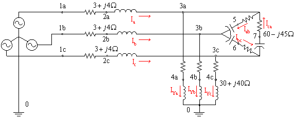
The Schematic and the Netlist are shown in
the following pages. The output files contain the following values for the
magnitude and phase angle of currents.
FREQ IM(V_PRINT1) IP(V_PRINT1)
6.000E+01 8.000E+00 -6.388E-05
FREQ IM(V_PRINT2) IP(V_PRINT2)
6.000E+01 8.000E+00 -1.200E+02
FREQ IM(V_PRINT3) IP(V_PRINT3)
6.000E+01 8.000E+00 1.200E+02
FREQ IM(V_PRINT7) IP(V_PRINT7)
6.000E+01 3.578E+00 -6.343E+01
FREQ IM(V_PRINT8) IP(V_PRINT8)
6.000E+01 3.578E+00 1.766E+02
FREQ IM(V_PRINT9) IP(V_PRINT9)
6.000E+01 3.578E+00 5.657E+01
FREQ IM(V_PRINT10) IP(V_PRINT10)
6.000E+01 4.131E+00 1.766E+02
FREQ IM(V_PRINT11) IP(V_PRINT11)
6.000E+01 4.131E+00 5.657E+01
FREQ IM(V_PRINT12) IP(V_PRINT12)
6.000E+01 4.131E+00 -6.343E+01
From
the above results the currents are:
(a) The line currents
,
(b) Currents in the Y-connected loads are:
,
(c) Currents in the D-connected loads are
,
* Schematics Netlist *
R_R1a 1a 2a 3
R_R1b 1b 2b 3
L_L1a 2a 5a 10.61mH
L_L1b 2b 5b 10.61mH
L_La4 4a 0 106.1MH
L_Lb4 4b 0 106.1mH
L_Lca 4c 0 106.1mH
R_Ra4 6a 4a 30
R_Rb4 6b 4b 30
R_Rc4 6c 4c 30
C_C5 8ca 3c 58.9463UF
R_R7 3c 7bc 60
L_L1c 2c 5c 10.61mH
R_R1c 1c 2c 3
V_Vc 1c 0 AC 200 -240
V_Va 1a 0 AC 200 0
V_Vb 1b 0 AC 200 -120
C_C6 8ab 3a 58.9463UF
R_R5 3a 7ca 60
C_C7 8bc 3b 58.9463UF
R_R6 3b 7ab 60
V_PRINT9 3c 6c 0V
.PRINT AC
+ IM(V_PRINT9)
+ IP(V_PRINT9)
V_PRINT1 5a 3a 0V
.PRINT AC
+ IM(V_PRINT1)
+ IP(V_PRINT1)
V_PRINT2 5b 3b 0V
.PRINT AC
+ IM(V_PRINT2)
+ IP(V_PRINT2)
V_PRINT3 5c 3c 0V
.PRINT AC
+ IM(V_PRINT3)
+ IP(V_PRINT3)
V_PRINT7 3a 6a 0V
.PRINT AC IM(V_PRINT7)
V_PRINT8 3b 6b 0V
.PRINT AC
+ IM(V_PRINT8)
V_PRINT10 8ca 7ca 0V
.PRINT AC
+ IM(V_PRINT10)
+ IP(V_PRINT10)
V_PRINT11 8ab 7ab 0V
.PRINT AC
+ IM(V_PRINT11)
+ IP(V_PRINT11)
V_PRINT12 8bc 7bc 0V
.PRINT AC
+ IM(V_PRINT12)
+
IP(V_PRINT12)
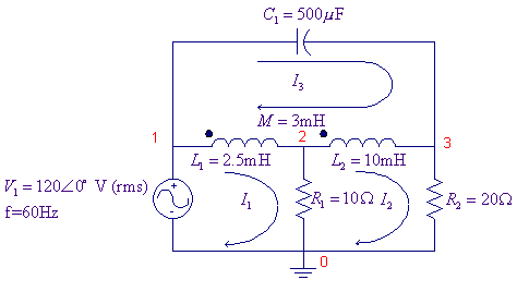
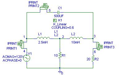
Mutually Coupled Circuits Determine the magnitudes and phase angles of mesh currents in
the coupled circuit shown.
PSpice uses the coupling coefficient to describe the coupled
coils, thus we find K from
The
“dot” convention for the coupling is related to the direction in which the
inductors are connected. The dot is always next to the first pin to be
netlisted. When the inductor symbol, L, is taken from the part library and is
placed without rotation, the “dotted” pin is the left one. Edit/Rotate
(<Ctrl R>) rotates the inductor +90deg, which makes this pin the one at
the bottom. The dotted terminal is always referred to the first node of the inductor
in the Netlist. So always examine the
net list and if the left node is not the dotted side, rotate the inductor in
the schematic until the desired dotted node is the first entry in the Netlist. The part K_linear can be
used to specify the mutual coupling between two or more inductors. The
parameters to be specified are L1, L2, … up to L6, whose values must be set to
the inductors symbols. The coupling value is the coefficient of mutual coupling, which must be specified between
zero and 1. The PSpice schematics
is as shown.
Three IPRINT symbols are inserted
in series in each loop to write the currents in the output file. In the text
box for each IPRINT set AC, MAG and PHASE to YES. From the analysis menu select
the Probe Setup, and disable the Probe. Enable the AC Analysis, select Linear, and set the Total pts to 1, Start
and End Frequencies to 60. Run PSpice
(Analysis, Simulate). The Schematics Netlist is as follows
L_L1 1 2 2.5mH
L_L2 2 3 10mH
C_C1 5 3 500UF
R_R1 2 0 10
V_PRINT3 3 6 0V
.PRINT AC
+ IM(V_PRINT3)
+
IP(V_PRINT3)
V_V1 4 0 DC
0V AC 120V 0
R_R2 6 0 20
Kn_K1 L_L1 L_L2 0.6
V_PRINT2 1 5 0V
.PRINT AC
+ IM(V_PRINT2)
+
IP(V_PRINT2)
V_PRINT1 4 1 0V
.PRINT AC
+ IM(V_PRINT1)
+ IP(V_PRINT1)
The output file contains the following values for the magnitude
and angles of the currents
FREQ IM(V_PRINT1) IP(V_PRINT1)
6.000E+01 1.164E+01 3.133E+01
FREQ IM(V_PRINT2) IP(V_PRINT2)
6.000E+01 2.438E+01 5.200E+01
FREQ IM(V_PRINT3) IP(V_PRINT3)
6.000E+01 4.083E+00 7.719E+01
From the above results, the mesh currents are:
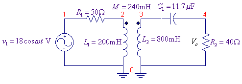
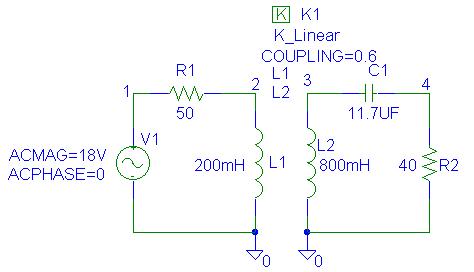
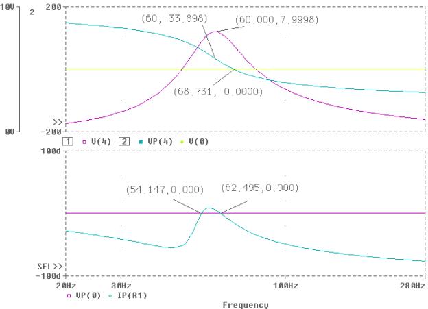
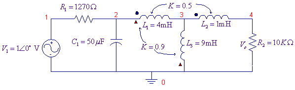
For the circuit shown, use PSpice and Probe to graph the magnitude and phase angle of the output voltage Vo, i.e., V(4) as a function of frequency. Use the AC analysis to sweep the source frequency linearly from 20 HZ to 280HZ in steps of 1HZ. Determine the frequency at which the amplitude of the output voltage Vo is a maximum; find the phase angle at this frequency. Also, find the frequency at which the impedance seen by the source is purely resistive.
First we calculate the coefficient of coupling
The PSpice Schematic is as shown.
The
Schematics Netlist is as follows:
Kn_K1 L_L1 L_L2 0.6
R_R1 1 2 50
R_R2 4 0 40
V_V1 1 0 DC 0V AC
18V 0
C_C1 3 4 11.7UF
L_L1 2 0 200mH
L_L2 3 0 800mH
Since the dotted terminal is always the first pin in the Netlist, L1 and L2 are rotated three
times such that their corresponding nodes are entered as 2 0, and 3 0 respectively.
In probe, Add Plot from the Plot menu to create two graphs on
the screen. Using Add from the Trace
menu plot V(4). From Plot use Add Y axis to create a new Y-axis, and add the
trace for voltage phase angle VP(4). Select Cursor from the Tools menu, select the Display and use Peak to
find the peak voltage. Use Label from the Tools menu and Mark the values at the
peak position. Switch the Cursor to
phase angle plot and Mark the values at the frequency corresponding to the peak
value. Switch to the lower graph and
use Trace to add the input voltage and the input current phase angles VP(1) and
IP(R1). Use Cursor and Mark to get the
frequencies at 0. The Probe result is as shown. From the graph the maximum
output voltage is V =
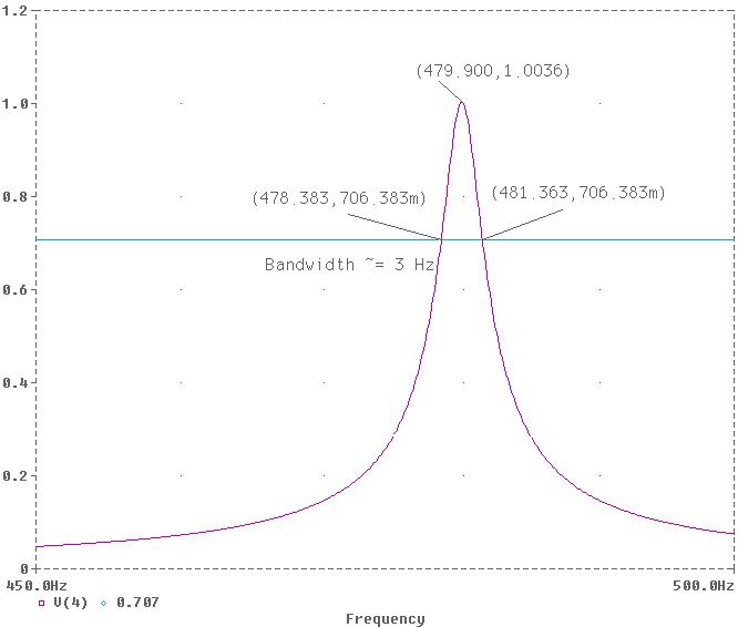
For the circuit shown, L1 and L2 are mutually coupled with a coupling coefficient of K = 0.5. Also, L1 and L3 are mutually coupled with a coupling coefficient of K = 0.9. Use PSpice and Probe to graph the magnitude of the output voltage Vo as a function of frequency. Use the AC analysis to sweep the source frequency
linearly from 450HZ to 500HZ in steps of 0.1HZ. Determine the frequency at which the amplitude of the output
voltage Vo is a maximum. If bandwidth is the frequency range within 0.707 of the peak value, find
the bandwidth.
Two K_linear parts are used to specify the mutual
coupling between L1, L2, and L1, L3. Since the dotted terminal is always
the first pin in the Netlist, L3 is
rotated once such that the corresponding nodes for L1 and L3 are entered as
2 3, and 0 3 respectively.
The PSpice Schematic is as shown.
The
Schematics Netlist is
L_L2 3 4 1mH
V_V1 1 0 DC 0V AC 1V 0
L_L1 2 3 4mH
R_R1 1 2 1270
C_C1 2 0 50UF
Kn_K1 L_L1 L_L2 0.5
R_R2 4 0 10K
Kn_K2 L_L1 L_L3 0.9
L_L3 0 3 9mH
Use Add from the Trace menu to plot V(4). From plot use the X_Axis Settings and set
the range from 450 Hz to 500 Hz. Select Cursor from the Tools menu, check the
Display and use Peak to find the peak voltage. Use Label from the Tools menu
and Mark the values at the peak position. Add a trace at 0.707 of the peak value. Use Cursor to Mark the corner frequencies at the intersection with the
0.707 line. Determine the bandwidth and Mark it on the graph. The probe result
is shown. From the graph the maximum
output voltage is
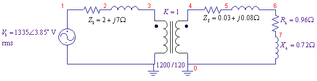
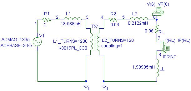
A 1200/120 V single-phase transformer has the following primary
and secondary winding impedances, HV winding:
From the given reactances at 60 HZ, the inductances are given by
.
We can use K3019PL non-linear core to model the
transformer, to model the ideal transformer the coupling coefficient is set to
1. The L1_Turns and L2_Turns values are
set to 1200 and 120 respectively. The PSpice Schematic is as shown.
The Schematics Netlist is
R_R2 4 5 0.03
L_L2 5 6 0.2122mH
R_R1 1 2 2
R_RL 6 7 0.96
L1_TX1 3 0 1200
L2_TX1 4 0 120
K_TX1 L1_TX1 L2_TX1 1 K3019PL_3C8
L_L1 2 3 18.568mH
L_LL 8 0 1.90985mH
V_V1 1 0 DC 0V AC 1335 3.85
.PRINT AC
+ VM([6])
+ VP([6])
V_PRINT2 7 8 0V
.PRINT AC
+ IM(V_PRINT2)
+ IP(V_PRINT2)
Double-click on the VPRINT1 symbol. Select 'SIMULATIONONLY=' and
for value type V(6) VP(6). In the text
box for VPRINT1 set AC, MAG and PHASE to YES. Also in the text box for IPRINT set AC, MAG and PHASE to YES. From the
analysis menu select the Probe Setup and disable the Probe. Enable the AC
Analysis, select Linear, and set the Total pts to 1, Start and End Frequencies
to 60. Run PSpice (Analysis, Simulate).
The output file contains the following values for the magnitude and phase angle
of currents.
FREQ VM(6) VP(6)
6.000E+01 1.200E+02 3.730E-04
FREQ IM(V_PRINT2) IP(V_PRINT2)
6.000E+01 1.000E+02 -3.687E+01
That is,
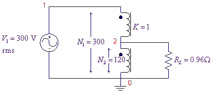
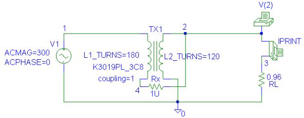
A 300/120V ideal autotransformer is supplying a load
We can use K3019PL non-linear core to model the transformer, to
model the ideal transformer the coupling coefficient is set to 1. For L1_Turns, we use
The Schematics Netlist is
L1_TX1 1 4 180
L2_TX1 2 0 120
K_TX1 L1_TX1 L2_TX1 1 K3019PL_3C8
V_V1 1 0 DC 0V AC 300 0
R_RL 3 0 0.96
.PRINT AC
+ VM([2])
V_PRINT2 2 3 0V
.PRINT AC
+ IM(V_PRINT2)
R_Rx 4 2 1U
Double-click on the VPRINT1 symbol.
Select 'SIMULATIONONLY=' and for value type V(2). In the text box for VPRINT1
set AC and MAG to YES. Also in the text
box for IPRINT set AC and MAG to YES. From the analysis menu select the Probe
Setup and disable the Probe. Enable the
AC Analysis, select Linear, and set the Total pts to 1, Start and End
Frequencies to 60. Run PSpice
(Analysis, Simulate). The output file contains the following values:
FREQ VM(2)
6.000E+01 1.200E+02
FREQ IM(V_PRINT2)
6.000E+01 1.250E+02
That is, VL = 120 V, and IL = 125 A.
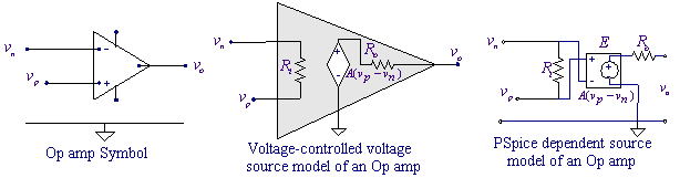
Operational
Amplifiers
The operational amplifier (called op amp) is an
electronic device that has become a versatile network element. The main
characteristics of an op amp are very high input resistance, very low output
resistance, and very high gain (to the order of 105). By focusing on
the terminal behavior of an op amp, one can appreciate its use as a network
element without knowledge of its internal behavior. The PSpice evaluation version has only one op amp (UA741), and
only two of these can be used before reaching the component limits. If you have a circuit with a large number of
op amps, you will be forced to use ideal op amps in the evaluation version. The
op amp may be modeled as a linear amplifier to simplify the design and analysis
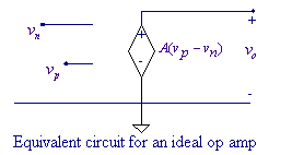
of op amp circuits. A
voltage-controlled voltage source can be used to model an op amp in the linear
range with reasonable accuracy as shown in the Figure below.
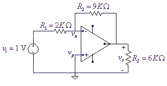
For the circuit shown below assume an ideal op
amp and use Spice to calculate the voltage gain
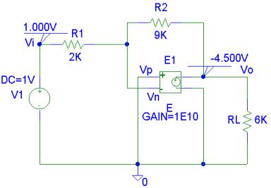
A voltage-controlled voltage source (Part E) is
used. The voltage gain is set to 1E10. The input and output node voltages are viewed using the VIEWPOINT part. The PSpice schematic containing the
simulation result is as shown below.
Schematics Netlist is
V_V1 Vi 0 DC 1V
E_E Vo 0 0 Vn 1E10
R_R2 Vn Vo 9K
R_RL Vo 0 6K
R_R1 Vi Vn 2K
Thus the voltage gain is -4.5.
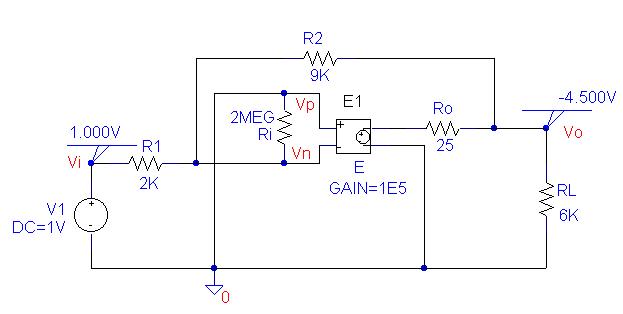
For Example 9 use a more realistic model with
the following parameters
The PSpice schematic containing the simulation
result is as shown below.
Schematics Netlist is
R_RL Vo 0 6K
V_V1 Vi 0 DC 1V
R_R1 Vi Vn 2K
R_Ri Vn 0 2MEG
E_E $N_0001 0 0 Vn 1E5
R_R2 Vn Vo 9K
R_Ro $N_0001 Vo 25
Thus the voltage gain is = -4.5 V approximately the same as the ideal
op amp model.
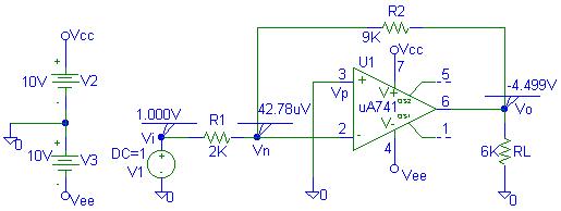
For Example 10 use a UA741 op amp. The op amp
positive power supply Vcc = 10 V, and the negative power
supply is Vee = 10 V. Two parts named BUBBLE are connected to
the supply nodes. Click on each BUBBLE to name these terminals Vcc and Vee. Two DC
supply of 10 V with BUBBLES named Vcc, and Vee are made as shown to provide the necessary voltages for terminal 7 and 4 of the
op amp. The PSpice schematic containing
the simulation result is as shown below.
Schematics Netlist is
R_R1 Vi Vn 2K
R_R2 Vn Vo 9K
V_V3 0 Vee 10V
V_V2 Vcc 0 10V
X_U1 0 Vn Vcc Vee Vo uA741
V_V1 Vi 0 DC 1
R_RL Vo 0 6K
Thus the voltage gain is = -4.499 compared to -4.5 obtained with the
ideal op amp model.
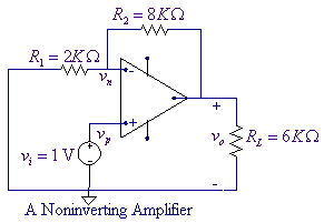
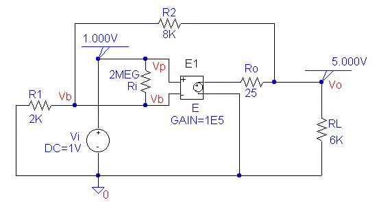
Determine the voltage gain in the noninverting
amplifier circuit shown. The amplifier parameters are
The PSpice schematic containing the simulation
result is as shown below.
The Schematics Netlist is
V_Vi Vp 0 DC 1V
R_Ri Vb Vp 2MEG
R_R1 0 Vb 2K
E_E $N_0001 0 Vp Vb 1E5
R_R2 Vb Vo 8K
R_Ro $N_0001 Vo 25
R_RL Vo 0 6K
Thus, the voltage gain is
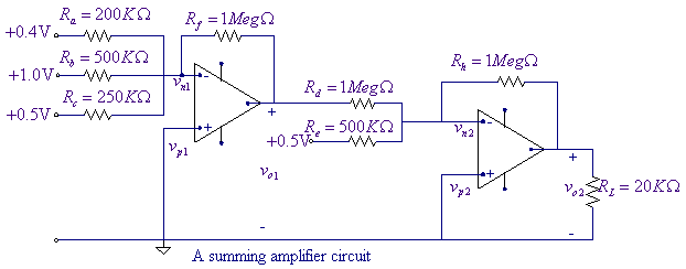
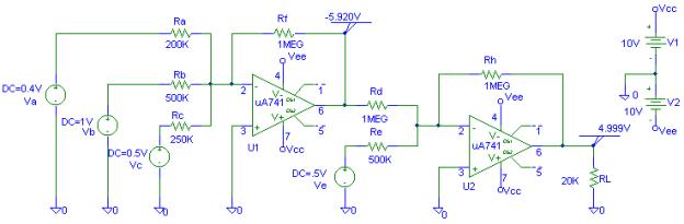
Example 13 (EE230Ex13.sch,
EE230Ex13b.sch) In the circuit shown below, determine
(a) Use two UA741 op amps. The op amp positive power supply Vcc = 10 V, and the negative power supply is Vee = 10 V.
The PSpice schematic containing the simulation
result is as shown below.
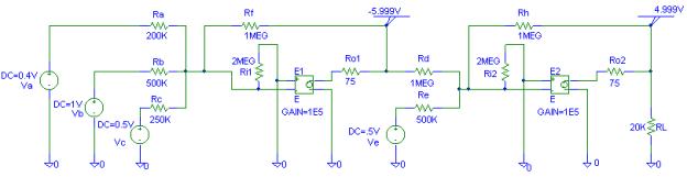
(b) Use to voltage-controlled voltage source to
model the op amps. The parameters of each op amp are
The PSpice schematic containing the simulation
result is as shown below. (EE230Ex13b.sch)
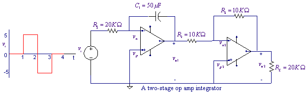
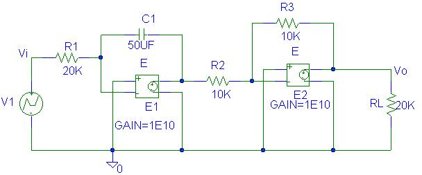
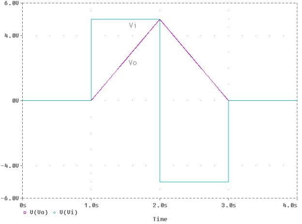
The source voltage in the circuit shown uses the
PSpice VPWL function to generate a waveform that is zero from 0 to 1 second,
jumps to +5 at t = 1 second, jump down to -5 at t = 2 second, jumps back to
zero at t = 3 seconds and remains at zero. The first op amp is an inverting integrator. The second op amp is a unity gain inverter. The overall circuit is a noninverting
integrator with a gain of
The output is the integral of the input as shown
below. Appling KCL at the inverting node, we get
For an ideal op amp Since the second op amp is a unity gain
inverter, we have
Substituting for
Two voltage-controlled voltage sources with
gains of 1010 are used to represent the ideal op amps. The PSpice schematic is as shown.
The Transient analysis is used to simulate the
circuit over a period of 4 seconds. The
Probe is used and the graph containing
|